Educational Sessions
Sunday, 13 April
9:00 am-4:45 pm
Educational Session 1: Mastering LLMs: A Deep Dive into Software Models, Hardware Challenges, Security and Reliability
The rapid advancements in large language models (LLMs) like Transformers have revolutionized artificial intelligence, driving significant interest in hardware accelerator design to meet their computational demands. However, as a hardware engineer, do you ever feel limited in your ideas due to a lack of software model knowledge? This educational session addresses this challenge by diving into the software architecture of Transformer models, offering insights into their fundamental building blocks, including quantization impact, the softmax bottleneck, multi-headed attention mechanisms, and variations of Transformer models. By understanding these critical aspects, hardware engineers will gain a deeper understanding of the unique challenges and opportunities posed by LLM models. The session aims to bridge the gap between LLM software models and hardware design, empowering engineers to brainstorm innovative circuit solutions that address these challenges effectively.
Session Chairs: Shanshan Xie, Intel & Prof. Yoonmyung Lee, Dept. of Electrical and Computer Engineering, Sungkyunkwan University
Dr. Paul Whatmough, Qualcomm, USA
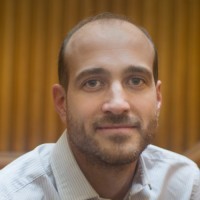 Bio: Paul N. Whatmough is Senior Director of AI Research at Qualcomm Inc., based in Cambridge, MA, USA. He received the Ph.D. degree from University College London, U.K., in 2012 and was previously head of Arm ML Research Lab. He is also a part-time Associate of the Harvard School of Engineering and Applied Sciences. He coauthored the book Deep Learning for Computer Architecture (Morgan & Claypool, 2017).
Title: Enabling Generative AI on Mobile SoCs using Hardware-Model Co-Design
Abstract: Generative AI models have introduced unprecedented new capabilities, generating incredible text, images and even video. However, this new breed of neural networks poses numerous challenges for edge devices, stressing both compute and memory system performance. In this tutorial, I will discuss the latest Generative AI networks and the challenges they pose for the hardware system, along many approaches proposed to help close the power and performance gap on mobile devices.
Dr. Debabrata Mohapatra, Meta, USA
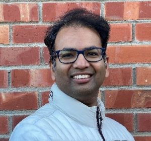 Bio: Debabrata Mohapatra earned his PhD in Electrical and Computer Engineering from Purdue University in 2011, advised by Prof. Kaushik Roy and Prof. Anand Raghunathan. He is a ML research scientist at Meta Reality Labs. Previously, he worked at Intel Labs on ML/CV hardware accelerators. His interests include efficient AI leveraging cross-domain optimizations.
Title: Deploying LLMs on the Edge: A HW/SW Co-Design Perspective
Abstract: Running large language models (LLM) on resource constrained edge devices is extremely challenging due to their sheer scale. In this talk, we discuss key considerations for the efficient on-device deployment of LLMs. We focus on understanding the software aspects of LLMs starting with basic transformer architecture, analyzing model compute and memory requirements, how techniques such as quantization, compression, sparsity can improve efficiency and finally how HW/SW co-design can help address some of these open challenges.
Dr. Tianlong Chen, Assistant Professor at The University of North Carolina at Chapel Hill, USA
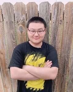 Bio: Dr. Chen is an assistant professor at CS@UNC Chapel Hill. His research spans efficient and reliable machine learning, multi-modal learning, and AI4Science. He has received a few Best Paper Awards from LoG’22, GenAI4Health@NeurIPS’24, Medicine and Healthcare Bridge@AAAI’25, Cisco Faculty Award, CPAL/AdvML Rising Star, and several PhD fellowships.
Title: Breaking the Resource Monopoly from Industries: Sustainable and Reliable LLM Serving By Recycling Outdated and Resource-Constrained GPUs
Abstract: Recently, LLM agents, exemplified by models like ChatGPT, have showcased remarkable prowess in various tasks, owing to their vast number of parameters and emergent in-context learning capabilities. To serve these gigantic models with billions of parameters is a trend. It becomes a must to explore how to use the existing hardware, especially outdated hardware, to collectively improve environmental sustainability, efficiency, and reliability for LLM serving. In this talk, I will traverse a series of contributions to efficient deep learning, particularly emphasizing modularized LLM architecture (Part 1), in-storage sustainable computing (Part 2), and reliable serving against software and hardware attacks (Part 3).
Prof. Xiaozhong Liu, Associate Professor at Worcester Polytechnic Institute, USA
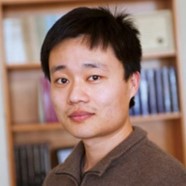 Bio: Dr. Xiaozhong Liu, an Associate Professor at WPI, specializes in NLP, LLM, retrieval, and deep learning, with a focus on LLM memorization, explainability, reasoning, and data heterogeneity. He has previous industry experience at Alibaba DAMO Academy and Yahoo.
Title: LLM Innovation with User Data
Abstract: This talk explores innovative approaches to enhancing LLM performance with user data. It will delve into novel models, including LLM memorization, personalization, knowledge-based reasoning, reinforcement learning strategies, and human-in-the-loop techniques, while examining how to efficiently harness user feedback. The presentation also highlights practical experiments in both general and specialized domains such as healthcare and legal, providing insights into next-generation LLM design and application.
Educational Session 2: High Precision Converters and Digital Calibration Techniques
Session Chairs: Prof. Shaolan Li, Georgia Institute of Technology & Dr. Yong Liu, Broadcom Inc.
High-resolution ADCs are key system building blocks in the era of Internet-of-Things and Artificial Inteligence, playing the role of capturing sensor signals, facilitating communication, as well as assisting high-performance computing. This educational session will focus on the most popular trends in recent year’s high-resolution ADC development.
Prof. Xiyuan Tang, Peking University, China
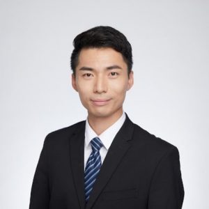 Bio: Dr. Tang is currently an assistant professor at Peking University. Xiyuan received the B.Sc. degree (Hons.) from the School of Microelectronics, Shanghai Jiao Tong University, Shanghai, China, in 2012, and the M.S. and Ph.D. degree in electrical engineering from The University of Texas at Austin, Austin, TX, USA, in 2014 and 2019 respectively. From 2014 to 2017, he was a Design Engineer with Silicon Laboratories, Austin, TX, where he worked on the RF receiver design. He was a postdoctoral researcher at the University of Texas at Austin from 2019 to 2021. Dr. Tang is a Senior Member of IEEE. He serves on the Technical Program Committees (TPC) of ISSCC. He also serves as an associate editor for IEEE Solid-State Circuits Letters. He was a recipient of IEEE Solid-State Circuits Society Rising Stars in 2020.
Title: Noise-Shaping SAR ADCs: From Fundamentals to Recent Advances
Abstract: Emerging over the past decade, noise-shaping (NS) SAR ADCs have rapidly become one of the most prominent architectures in the ADC landscape. By combining the advantages of both SAR and ΔΣ modulator architectures, NS-SAR offers remarkable potential for high efficiency, low cost, and scalability with continued process advancements. This talk will begin by introducing the basic principles of noise-shaping SAR ADCs, highlighting the key challenges. Then, the main NS-SAR architectures will be discussed, followed by an exploration of the latest advancements, such as advanced loop filtering, DAC mismatch mitigation, and speed enhancement techniques. Finally, the talk will provide a comparison of state-of-the-art NS-SAR ADCs and outline promising future research directions.
Prof. Minkyu Je, Korea Advanced Institute of Science and Technology, South Korea
 Bio: Minkyu Je received his B.S., M.S., and Ph.D. from KAIST. He worked at Samsung Electronics, IME A*STAR, and DGIST before becoming an Associate Professor at KAIST. His research focuses on IC platforms for smart sensors, wireless communication, and biomedical devices. He holds 80+ patents and has 430+ publications.
Title: ADC Architectures and Techniques for Biomedical and Sensor Interfaces
Abstract: Recent advancements in IoT and biomedical systems have increased the demand for optimized front-end architectures in sensor readout applications. Sensors convert physical quantities into electrical signals such as resistance, capacitance, voltage, and current, requiring a dedicated ADC architecture to meet the specific requirements of each sensor interface. In this talk, the fundamental structures of sensor interfaces and their corresponding ADC architectures and design techniques will be introduced. Then, the diverse applications across biomedical and environmental sensing with key parameter trade-offs will be presented, offering insights into emerging trends and future research directions in ADC development for sensor interfaces.
Prof. Nima Maghari, University of Florida, USA
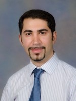 Bio: Nima Maghari received his B.S. from the University of Tehran (2004) and Ph.D. from Oregon State University (2010). He is an Associate Professor at the University of Florida. His research focuses on high-performance ADCs, delta-sigma modulators, synthesizable analog circuits, and analog security. He has 70+ IEEE publications and serves on multiple technical committees.
Title: Continuous-Time Delta-Sigma Modulators Architectures
Abstract: Delta-Sigma modulators are extensively utilized in applications ranging from low-frequency audio to wideband wireless receivers. Their success can be attributed to several key advantages, including effective anti-aliasing filtering, reduced sensitivity to circuit non-idealities (such as lower requirements for op-amp gain), and a wide dynamic range. However, as the demand for higher data rates and wide bandwidth increases, the sampling speed becomes a limiting factor for delta-sigma ADCs in maintaining efficient oversampling ratios. The rise of Continuous-Time Delta-Sigma Modulators (CTDSMs) marks a significant shift in the system-level design of these structures. Traditional multi-stage noise-shaping techniques struggle with large RC variations, while single-loop designs face challenges related to reduced dynamic range. In this talk, we will delve into the fundamentals of DSM operation, examine the advantages and drawbacks of CTDSMs, and discuss new innovative architectures.
Dr. Huseyin Dinc, ADI, USA
 Bio: Huseyin Dinc received the Ph.D. degree from Georgia Institute of Technology. Dr. Dinc has been with Analog Devices Inc., specializing in high-speed pipelined ADCs since 2008. He was the co-recipient of the 2020 ISSCC Outstanding Paper Award. His technical interests include digitally-assisted analog-circuit design, and low-distortion and low-noise circuits.
Title: Digital Calibration Techniques for High-Speed Pipelined ADCs
Abstract: The design of high-speed pipelined analog-to-digital converters required for demanding applications is only possible with background calibration of many impairments inherent in analog circuits. While leveraging background calibrations has simplified the architecture and design of analog circuits leading to substantial speed improvements and power savings, relying on such calibrations has resulted in considerable complexity. In this talk, we will go over several calibration techniques, and touch on strategies for managing complexity, portability, and minimizing power.
Educational Session 3: Security or Privacy From Hardware to Systems
Session Chairs: Mingu Kang, University of California San Diego & Dr. Kevin Tien, IBM T. J. Watson Research Center
This session explores cutting-edge hardware security solutions, from attack-resistant cryptographic accelerators that counter side-channel and fault-injection threats to zero-trust architectures extending trusted execution environments (TEEs) to AI accelerators and chiplet-based designs. Additionally, we discuss AI-enabled edge devices with on-chip sensors that autonomously detect and respond to attacks. Together, these talks offer insights into building resilient, secure platforms for the future of computing.
Dr. Sandhya Koteshwara, IBM, USA
 Bio: Dr. Sandhya Koteshwara is a Staff Research Scientist at IBM T.J. Watson Research Center in Yorktown Heights, New York. She is currently working in the cloud infrastructure department on security and performance of IBM’s AI accelerators. Dr. Koteshwara graduated from the University of Minnesota with a doctorate degree in Electrical and Computer Engineering in 2018. She has authored several papers and patents and has been selected as a Young Researcher at Heidelberg Laureate Forum 2018, participant of the Rising Stars in EECS 2017 and is a recipient of the SRC Mahboob Khan Outstanding Liaison Award 2023.
Title: Bringing the zero-trust model to hardware: From systems to silicon
Abstract: In recent times, there has been a major push and urgency to adopt the zero-trust model for cybersecurity. The zero-trust model is based on the principle of “never trust, always verify” and is aimed at eliminating all implicit trust in a system. While adopting a zero-trust model for network security generally involves authenticating, authorizing and continuously validating the credentials of users in a network, these measures need to be modified and extended to create underlying hardware that is trusted and secured. Thus, novel approaches for building zero trust architectures, from systems all the way down to silicon, is one of the big challenges for next generation secure hardware system design.
In this talk, we will start at the system level by understanding how security and trust have been traditionally built into host systems. We will understand the concept of a hardware “Root of Trust” which is the anchor of trust in these systems and from which trust is extended to all components. As an integral part of this trusted system, AI accelerators should be designed with security in mind. I will present our work on extending Trusted Execution Environments or TEEs to accelerators such as TPUs/AIUs. In the second half of the talk, we will dive deeper into silicon and explore the challenges and opportunities of bringing zero-trust to heterogeneous integration or System-in-Package based designs which rely on chiplet technology.
Mr. Sanu Mathew, Intel Corporation, USA
 Bio: Sanu Mathew is a Senior Principal Research Scientist with the Circuits Research Labs, Intel Labs, of Intel Corporation, Hillsboro, OR, where he is leads the security and arithmetic circuits team. His research work specializes in the areas of highspeed/low power computer arithmetic data-path circuits and special-purpose accelerators for cryptography and security. He received the B.Tech. degree in Electronics Engineering from College of Engineering, Trivandrum, India in 1993, followed by M.S and Ph.D. degrees in Electrical Engineering from State University of New York at Buffalo in 1996 and 1999 respectively. He holds 100 issued patents, has 35 patents pending with over 105 conference/journal publications. Sanu is a Fellow of the IEEE.
Title: Attack-Resistant Crypto Hardware Accelerators for Secure Platforms
Abstract: Secure platforms rely on silicon-embedded root-of-trust circuits to deliver security guarantees, while operating in hostile environments where adversaries are present at all layers of the compute stack. Attackers employ a variety of attack modalities using side-channels (SCA) and fault-injection (FIA) to steal on-die secret keys/IDs. In this tutorial, we will discuss how attackers mount SCA and FIA on symmetric-key encryption engines and explore first-order countermeasures against such attacks, while minimizing the area, power and performance overheads. The tutorial will describe the design of a reconfigurable AES engine that operates in SCA-resistant mode in a hostile environment, while allowing the administrator to switch to a high-performance mode while operating in a secure environment. We will also discuss the design of a self-checking AES engine that detects malicious injected faults in real-time using checker circuits.
Prof. Kaiyuan Yang, Rice University, USA
 Bio: Kaiyuan Yang is an Associate Professor of Electrical and Computer Engineering at Rice University, USA, where he leads the Secure and Intelligent Micro-Systems (SIMS) lab. He received his B.S. degree in Electronic Engineering from Tsinghua University, China, in 2012, and his Ph.D. degree in Electrical Engineering from the University of Michigan – Ann Arbor, in 2017. His research interests include low-power integrated circuits and system design for secure and intelligent microsystems, bioelectronics, hardware security, and mixed-signal computing. He is a recipient of the NSF CAREER Award, IEEE SSCS Predoctoral Achievement Award, and best paper awards from premier conferences in multiple fields, including 2024 IEEE EMBC, 2022 ACM MobiCom, 2021 IEEE CICC, 2016 IEEE S&P, and 2015 IEEE ISCAS. His research was recognized as the research highlights of Communications of ACM (CACM), ACM GetMobile, and IEEE Top Picks in Hardware and Embedded Security. He is currently an associate editor of IEEE Transactions on VLSI Systems (TVLSI), a program committee member of ISSCC, CICC, and ISCA conferences, and a member of SSCS Solid-State Circuits Directions (SSCD) committee.
Title: Securing Ubiquitous Devices with Ultra-Lightweight Circuit Primitives
Abstract: Security and privacy are critical challenges to overcome in ubiquitous electronics, such as IoT and wearable/implantable devices. Securing these systems faces not only new challenges at system and network levels due to a vast variance of applications, system constructions, and attack surfaces, but also severe hardware resource constraints on computation resources, power consumption, and device cost. To tackle these challenges, significant research efforts have been pursuing specialized hardware-enabled security primitives that could help build a reliable, trustful, and energy-efficient foundation for system security. This tutorial will give an overview of the problems and focus on three hardware security challenges that could be dealt with through novel circuit designs, namely entropy generation, countermeasures against side-channel and fault-injection attacks, and lightweight computing for edge security. I will review state-of-the-art circuit-enabled security primitives, including our recent work towards all-digital, fully synthesizable, and compact circuit techniques that enable agile SoC development and technology portability. Novel circuit principles that cross the boundary of traditional digital and analog designs have significantly improved the performance and overheads of these security primitives.
Prof. Massimo Alioto, Department of Electrical and Computer Engineering, National University of Singapore, Singapore
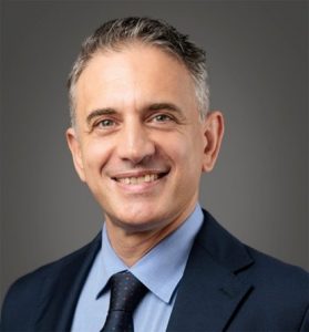 Bio: Massimo Alioto is Provost’s Chair Professor at the National University of Singapore, and leads the Green IC group among the others. He held positions at the University of Siena, Michigan (Ann Arbor), California (Berkeley), Intel Labs, EPFL. He authored 400 publications, 5 books and 30 patents. His research interests include widely energy-scalable systems, self-powered and green wireless systems, data-driven silicon systems, and hardware security, among the others. He was IEEE TVLSI Editor in Chief and IEEE JETCAS Deputy Editor in Chief, Distinguished Lecturer for CAS and SSC Society, and is the Chair of the DLP program for CAS Society. He was Guest Editor in several IEEE journals (JSSC, TCAS-I, JETCAS) and best paper award recipient (e.g., ISSCC). Prof. Alioto is an IEEE Fellow.
Title: Reuse-Centric Design for Ubiquitous Hardware Security – From Circuits to Machine Learning Algorithms
Abstract: The rapidly increasing attack surface of connected devices and the decreasing cost of hardware security threats now demand ubiquitous deployment of security countermeasures down to edge silicon systems. In this tutorial, the on-going and prospective evolution of hardware security is observed through an original macro-trend analysis, and the coverage of recent and promising directions to protect confidential information/data in intelligent sensors (e.g., on-chip AI model) from network down to physical level. As emerging security trend towards more self-reliant edge devices, on-chip intelligent sensors with built-in AI to autonomously detect and respond to attacks are finally discussed.
Educational Session 4: Advanced Biomedical Interfaces
Session Chairs: Prof. Constantine Sideris, University of Southern California & Dr. Yaoyao Jia, The University of Texas at Austin
Prof. Hyung-Min Lee, Korea University, South Korea
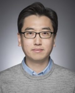 Bio: Hyung-Min Lee received the Ph.D. degree from Georgia Institute of Technology in 2014. He was with the Massachusetts Institute of Technology as a Post-Doctoral Researcher (2014-2015) and the IBM T. J. Watson Research Center as a Research Staff Member (2015-2017). In 2017, he joined the School of Electrical Engineering, Korea University, where he is currently an Associate Professor. His research area includes analog/mixed-signal IC and microsystem design for biomedical, sensor, power management, display/touch, and neuromorphic applications. He was a co-recipient of the IEEE CICC Outstanding Student Paper Award in 2023 and IEEE SSCS-Brain Best Paper Award in 2024. He currently serves as an Associate Editor of IEEE TBioCAS and OJCAS. He is a TPC member of ISSCC.
Title: Efficient and Effective Implantable Neural Stimulation: Challenges and Circuit Solutions
Abstract: Implantable medical devices (IMD) with neural stimulating functions have been proven as effective therapies to alleviate neurological diseases or substitute sensory modalities, while requiring large energy and high performance for more efficacious treatments. These IMDs also contribute to the development of brain-machine interface, closed-loop neuromodulation, and neural prosthesis that can sense, control, and connect the brain to the external world. However, stimulation performance is significantly affected by several factors in IMDs, such as size constraints, limited power source, low efficiency/efficacy, insufficient compliance voltage, safety issues, etc. Therefore, implantable neural stimulation still requires more aggressive circuit techniques to further improve overall energy efficiency, while ensuring precise, safe, and effective functions. In this talk, I will present various challenges and circuit solutions for efficient and effective implantable neural stimulation in both electronic and biological aspects.
Prof. Dante Gabriel Muratore, Delft University of Technology, Netherlands
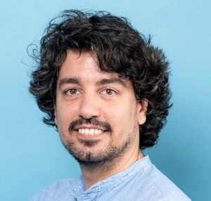 Bio: Dante G. Muratore received a Ph.D. degree in Microelectronics from the University of Pavia in 2017. He was a Visiting Scholar at MIT and a Postdoctoral Fellow at Stanford University. Since 2020, he is an assistant professor at Delft University of Technology, where he leads the Smart Brain Interfaces group. His group investigates hardware and system solutions for high-bandwidth brain-computer interfaces that can interact with the nervous system at natural resolution. They contribute solutions for recording and stimulation circuits, on-chip neural signal processing, and wireless power and data transfer.
Title: On-chip signal processing and compression for brain-computer interfaces
Abstract: Autonomous interfaces to the brain that can operate at the natural resolution and scale of the nervous system will open up stunning possibilities for a range of biomedical applications and may eventually be the basis for augmentation of natural human capabilities. These interfaces generate a massive amount of raw data that needs to be processed on the chip before being transmitted outside the implant to enable fully wireless operation. In this session, we will cover the basics of brain-computer interfaces and the related neural signals before diving into advanced mixed-signal and digital accelerators for neural signal processing and compression. We will discuss the challenges associated with power/area constraints and the need to operate in real time. Then, we will cover examples of ML-based classifiers, spike-sorting accelerators, mixed-signal compressive readouts, neuromorphic processors, and more. Finally, we will discuss the challenges and opportunities in IC design for the next generation of implantable brain interfaces.
Prof. Mehdi Kiani, Penn State University, USA
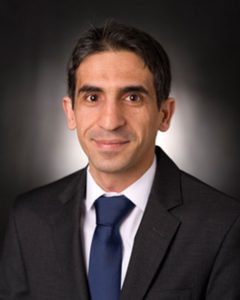 Bio: Mehdi Kiani received his Ph.D. degree in Electrical and Computer Engineering from the Georgia Institute of Technology in 2014. He joined the faculty of the School of Electrical Engineering and Computer Science at the Pennsylvania State University in August 2014 where he is currently an Associate Professor. His research interests are in the multidisciplinary areas of analog and power-management integrated circuits, ultrasound-based medical systems, wireless power transfer, implantable medical devices, and neural interfaces. He was a recipient of the 2020 NSF CAREER Award. He is currently an Associate Editor of the IEEE Transactions on Biomedical Circuits and Systems and Journal of Neuroelectronics. He serves as the technical program committee member of the IEEE International Solid-State Circuits Conference in the medical subcommittee.
Title: Wireless Power Transfer to Implantable Medical Devices
Abstract: Wireless technologies are essential to the advancement of modern biomedical systems, enabling innovative solutions for healthcare monitoring, diagnostics, and treatment. One of the rapidly growing areas in this field is implantable medical devices (IMDs), which rely on wireless technology for communication, control, and power delivery. As IMDs continue to shrink in size and expand in functionality, efficient and reliable wireless power transfer (WPT) becomes increasingly critical to their success. This talk will explore state-of-the-art WPT techniques tailored for IMDs, with a focus on various modalities suited for millimeter-scale implants. Key topics will include the fundamental principles of WPT, recent advancements, and novel strategies for overcoming challenges such as miniaturization constraints, misalignments, and safety considerations.
Prof. Jerald Yoo, Seoul National University, South Korea
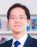 Bio:Jerald Yoo is a Professor of Electrical and Computer Engineering at Seoul National University. He received his Ph.D. degree in Electrical Engineering from KAIST, Korea in 2010. Between 2010 and 2024, he worked at Massachusetts Institute of Technology (visiting scholar), Masdar Institute of Science and Technology, Abu Dhabi, UAE (now Khalifa university), and National University of Singapore. He has pioneered research on low-energy body-area-network (BAN) transceivers and biomedical circuits and systems. Dr. Yoo served as a Distinguished Lecturer for IEEE Circuits and Systems Society (CASS) (2019-2021) and for IEEE Solid-State Circuits Society (SSCS) (2017- 2018/2024-2025). He has served as TPC member of ISSCC, VLSI Symposium, CICC
(ETA Subcommittee chair), A-SSCC (Emerging Technologies Subcommittee Chair) and ISLPED (General co-chair/TPC co-chair).
Title: Wearable e-health: from electrodes to signal processing and powering
Abstract: Wearable eHealth targets to mitigate the impact of chronic diseases by providing continuous yet adequate monitoring and analysis of physiological signals. However, the wearable environment is challenging for circuit designers due to its unstable skin-electrode interface, huge mismatch, and static/dynamic offset. Also, in system perspective, trade-off between available resource and performance among the components (analog front-end and digital back-end) is of crucial. This talk will cover the design strategies of wearable eHealth System-on-Chip (SoC). We will check how to set the right system design goal. We will then explore the difficulties, limitations and potential pitfalls in wearable interface circuit design, and strategies to overcome such issues. Several state-of-the-art sensor interfaces that emphasize different parameters will be discussed. Moving on, we will investigate the feature extraction and the patient-specific classification using on-chip Machine Learning technique. Finally, an on-chip patient-specific epilepsy detection System-on-Chip (SoC) will be presented, which integrates all the components covered during the talk. The talk will conclude with interesting aspects and opportunities that lie ahead, including powering the wearables.
