CICC 2025 Panel Sessions
Monday, 14 April
1:30 pm-3:00 pm
Do we really need a linear-gain amplifier anymore?
Traditionally, integrated circuits rely heavily on linear gain amplifiers to boost voltage levels and power levels of analog signals. Requirements for these amplifiers include sufficiently low noise and distortion levels, sufficient signal bandwidth and decent input and output impedances, all for a sufficiently low power and area budget.
With newer (smaller) technology nodes, minimum length transistors get faster and less ideal while their (maximum) supply voltage tends to reduce. This lower supply voltage more-than-proportionally reduces the voltage headroom in analog circuits which makes it increasingly hard to maintain or even improve the SNR and bandwidth for a fixed power budget. Running analog circuits from a (relatively) high supply voltage and using a mix-and-match of low-voltage and high-voltage (I/O) transistors in the same technology node may be leveraged to maintain performance for a fixed power and area budget. Likewise, a multi-die/single package solution where critical analog blocks are realized on dedicated dies may be used to implement a best-of-multiple-worlds overall-optimum solution.
Replacing linear analog amplifiers is done in just a few fields, most notably in class D, E, F and switched cap power amplifiers. It may be time to push towards solutions where we can ditch all linear amplifiers and replace them by digital-only, advanced CMOS compatible, circuitry.
Our panelists approach this issue from many angles: industrial, academic, fundamental, practical, at low(er) frequency, at RF, and many more. What is the best approach now, in the coming few years, or in the longer run? We invite you to enjoy the discussions and whenever possible to join the discussion!
Session Chairs: Anne-Johan Annema, University of Twente & Devrim Aksin, Analog Devices
Panelists:
Bram Nauta, University of Twente, The Netherlands
 Bio: Bram Nauta is a professor at the University of Twente, The Netherlands. He served as Editor-in-Chief (2007-2010) of the IEEE Journal of Solid-State Circuits (JSSC) and was the 2013 program chair of the International Solid-State Circuits Conference (ISSCC). He served as the President of the IEEE Solid-State Circuits Society (2018-2019 term).
Position Statement:
No 😉
Huseyin Dinc, Analog Devices Inc., Durhan, NC, USA
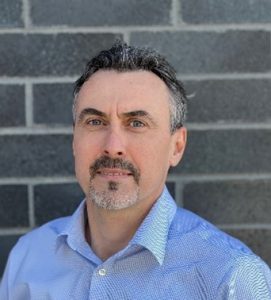 Bio: Huseyin Dinc received the Ph.D. degree from the Georgia Institute of Technology. Since 2008, he has been with Analog Devices Inc., specializing in high-speed pipelined ADCs. He was the co-recipient of the 2020 ISSCC Outstanding Paper Award. His technical interests include digitally-assisted analog-circuit design, and low-distortion and low-noise circuits.
Position Statement: As with most things in analog circuit design, there is no one-size-fits-all solution for meeting linearity requirements within the design constraints. The designer must make sound engineering decisions to satisfy the linearity requirements either by relying on proven all analog methods or where practical, by leveraging digitally-assisted techniques to simplify the analog design.
Ali Sheikholeslami, University of Toronto, Canada
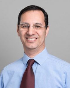 Bio: Ali Sheikholeslami is a professor of Electrical and Computer Engineering at the University of Toronto, Canada. His area of expertise are in analog, digital, and mixed-signal design for wireline applications. He is a co-author of a graduate-level textbook titled “Understanding Jitter and Phase Noise” and the author of Circuit Intuitions, a regular column series in the Solid-State Circuits Magazine.
Position Statement: Clinging to traditional analog amplifiers is holding us back from achieving the performance, scalability, and efficiency modern applications demand. It’s time to let analog, however nonlinear, handle amplification, while digital ensure linearity, paving the way for innovative mixed-mode solutions.
Swami Sankaran, Texas Instrument Inc., Dallas, TX, USA
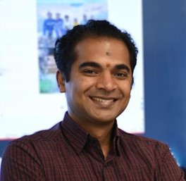 Bio: Swaminathan Sankaran Distinguished Member Technical Staff (DMTS) with Texas Instruments (TI), Dallas, Texas, USA directing RF and mmWave product and research activities spanning across design, validation and test. He has (Co)/(Director-ed)/Authored 25+/34 internal-TI/external-IEEE conference/journal papers winning multiple best industry-paper awards and holds >60 granted patents to-date. He has served as TPC member for ISSCC and as TPC-Fellow at CICC.
Position Statement: “Clocked-Amplifiers” are cool for publications and citation counts and perhaps have their space in systems with a) moderate link budgets, b) a defined sys-ref and c) appropriate frequency planning- They will not solve vast majority of existential problems. Multi-billion $, cost-commoditized/high-performance (sub 1-dB NF/36dBm+) catalog, mass-market amplifier space cannot afford the addition of a clock/associated in-band spurs/clock leakage.
Peter Kinget, Columbia, NY
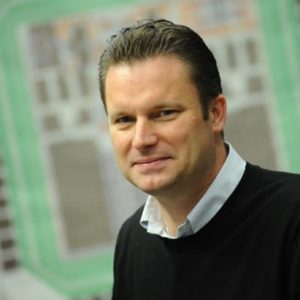 Bio: Peter Kinget is the Bernard J. Lechner Professor of Electrical Engineering at Columbia University in New York. He designs analog and RF integrated cir-cuits for novel applications in communications, sensing, or computing. He alsodevotes a lot of his energy to teaching initiatives like https://mosbius.org and https://vlsidesignlab.org
Position Statement: Most analog circuits interact with the real world. Maxwell equations in free space and many materials under practical conditions are astoundingly linear. Even if it’s hard to design linear electronic amplifiers, combatting noise requires linear amplification. To date, adding non-linearities in communications has been a fool’s errand especially in shared-channel, multi-user scenarios. Solving that is a system design challenge. Non-linearities are needed to make decisions and do computation, but digital owns that space. Or not?
Tuesday, 15 April
8:00 am-9:30 am
mmWave/THz Design: A New Paradigm or a Repeat of History with Faster Transistors?
For decades, wireless communications, radar, and sensing applications have driven the development of RF, mmWave, and now (sub-)THz IC design. Yet, if we take a closer look at core transceiver building blocks, their basic topologies have barely changed for almost 60 years. Even the phased array architecture that dominates today’s mmWave 5G radios traces its roots back to World War II. It appears the only real advancements have come from the increased transistor speed and lower cost of silicon fabrication and integration. Now in the post-Moore’s Law era where we have not seen significant RF transistor technology breakthroughs in nearly a decade, is the field of mmWave/THz IC design doomed to incremental stagnation? Are we just recycling the same ideas from decades ago? Is there room for a radical paradigm shift in high-frequency circuit topologies, transceiver architectures, and design methodologies? In this panel, five renowned experts will tackle these pressing questions head-on. Expect a lively debate and perhaps a glimpse of the next wave of true high-frequency circuit innovations.
Session Chairs: Dr. Mark Oude Alink, University of Twente, & Prof. Taiyun Chi, Rice University
Panelists:
Mark Rodwell, UC Santa Barbara, USA
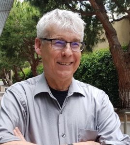 Bio: Mark Rodwell (Ph.D. Stanford 1988) holds the Doluca Family Endowed Chair in Electrical and Computer Engineering at UCSB. His research group develops high-frequency transistors, ICs and communications systems. He and his collaborators received the 2022 SIA-SRC University Researcher Award, the 2010 IEEE Sarnoff Award, the 2012 IEEE Marconi Prize Paper Award, the 1997 IEEE Microwave Prize, the 2009 IEEE IPRM Conference Award, and the 1998 European Microwave Conference Microwave Prize. For 2024-2025, he is serving as an IEEE-MTT-S Distinguished Microwave Lecturer.
Position Statement: Transistors have become smaller, faster, and cheaper, but, at a given frequency, it is hard to make tuning (energy storage) elements smaller, Ohm’s and Kirchoff’s laws haven’t changed, and reactive tuning for minimum noise measure or for maximum PAE has long been fully understood. Below 10 GHz, on-chip reactive tuning always will be painful, hence, long ago, discrete RF was better than RF-ICs; now, with higher-gain transistors, we can tune imperfectly, and still get good performance in a compact RF-IC. As we move above 100 GHz, RF-IC design is death by a thousand small cuts, with circuit gain, noise, and PAE all far poorer than transistor fundamental limits. Further, 100+ GHz links must use large arrays to offset propagation losses. It is all about picking circuits that minimize passive element losses, making faster transistors, and squeezing IC arrays into half-wave pitch.
Michael Thompson, Cadence, USA
 Bio: Michael Thompson is a Distinguished Engineer with Cadence Design Systems and part of the Virtuoso R&D team. Before moving to the EDA world, he worked in phased-array radars and radiometric sensor design and has deployed designs and systems from 2 GHz to 300 GHz. He holds a BSECE and MEE from Cal Poly, Pomona, with post-grad courses at USC in Antenna Theory.
Position Statement: The fundamental engineering and mathematics remain the same across the different frequencies of interest, but the medium of operation varies considerably and results in different distributive and parasitic considerations. Transmission line implementation in microstrip has other concerns than waveguide implementation. Layered on top of the medium used is the manufacturability and alignment of components at higher frequencies, where size limitations affect what can be produced or at least produced economically.
Kenichi Okada, Institute of Science Tokyo, Japan
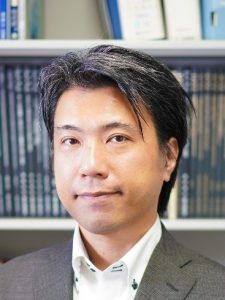 Bio: Prof. Kenichi Okada received the B.E., M.E., and Ph.D. degrees from Kyoto University, Kyoto, Japan, in 1998, 2000, and 2003, respectively. He joined Tokyo Institute of Technology in 2003, and he is now Professor in Institute of Science Tokyo. He has authored and co-authored more than 500 journal and conference papers. His current research interests include millimeter-wave/terahertz wireless transceiver, digital PLL, and ultra-low-power RF circuits. He is/was a TPC member of ISSCC, VLSI Circuits, ESSCIRC, RFIC Symposium, A-SSCC, Guest Editors and Associate Editors of JSSC and T-MTT, a Distinguished Lecturer of SSCS, and IEEE Fellow.
Position Statement: mmWave/THz design is not a repeat of history! The design difficulty/complexity of mmWave/THz arises from measurement accuracy and transistor performance. At frequencies exceeding 200 GHz, measurement inaccuracies make it challenging to refine simulation models. Without an accurate simulation model and reliable measurement, improving simulation accuracy becomes a terrible task. Actually, 60-GHz designs using the same 65nm bulk CMOS are quite different between now and 20 years ago. One more thing is that the ft/fmax of CMOS transistors is nearly saturated, at least when compared to the rate of increase in carrier frequency in CMOS wireless transceivers. Recently, the operating frequency has approached the ft/fmax, requiring different circuit techniques for the near-ft/fmax designs.
Bodhisatwa Sadhu, IBM, USA
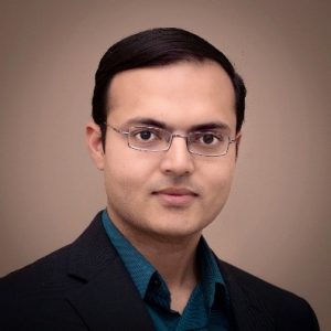 Bio: Bodhisatwa Sadhu is a Senior Research Scientist and Master Inventor at IBM T.J. Watson Research Center, NY. He has led several 5G phased array innovations, authored 70+ papers, 80+ patents, and a book, and won best paper awards at ISSCC, JSSC, and RFIC. He serves as JSSC Associate Editor, and RFIC Steering Committee Member.
Position Statement: While the fundamental design challenges have indeed scaled, design methodologies have evolved significantly making the designer experience vastly different.
Sorin Voinigescu, University of Toronto, Canada
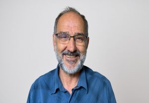 Bio: Sorin P. Voinigescu is a Professor in the Electrical and Computer Engineering Department at the University of Toronto where he holds the Stanley Ho Chair in Microelectronics and is the Director of the VLSI Research Group. He is an IEEE Fellow and an expert on millimeter-wave and atomic-scale semiconductor device technologies and their applications in quantum computing, mm-wave radar, radio and fibreoptic integrated circuits beyond 300 GHz and 300 GBaud.
Position Statement: Both. Millimeter-wave/THz circuit design, just like lower frequency analog mixed-signal and RF circuit design is algorithmic. At its core is the transistor. All things and other transistor FoMs being equal, faster transistors are mandatory for higher circuit performance. No amount of optimization and AI can compensate for higher transistor MAG and lower noise figure. What differentiates upper mm-wave/THz design is the importance of layout parasitics, especially in CMOS technology. At 300 GHz, unlike at lower frequencies, even a via inductance of 1-3 pH must be accounted for, capacitors are inductive, HBTs and cascodes are unstable. Circuit design is guided by transistor measurements above 100 GHz and starts simultaneously at top-level padframe layout and scalable transistor p-cell layout to minimize layout parasitics.
Tuesday, 15 April
10:05 am-11:35 am
Wireline and Lightwave Interconnects – The Shifting Boundary in the AI Era
In the rapidly evolving field of Artificial Intelligence (AI), the demand for high-performance computing infrastructure has reached unprecedented levels. Central to this infrastructure are the energy-efficient, high-bandwidth interconnects that enable rapid data exchange between servers and chips. This session will delve into the critical role of high-speed interconnects in AI servers, with a particular focus on the latest advancements in lightwave and wireline interconnect technologies.
Session Chairs: Win-san (Vince) Khwa, TSMC & Henry Park, MediaTek
Panelists:
Davide Tonietto, Huawei, Canada
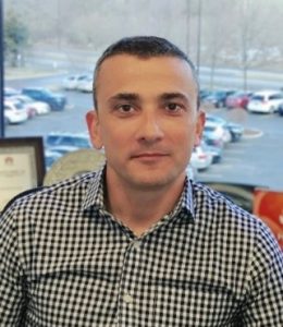 Bio: Huawei Fellow & Founder of Hisilicon Serial Link Team (A.K.A. HiLink), with Huawei Technologies Canada since 2011. Responsible for Hisilicon SerDes IP technology roadmap definition, execution and integration from 2011 to 2021. He holds more than 20 US patents and co-authored several papers on SerDes and wireline communication. His current focus is on improving interconnect efficiency by increasing parallelism and decreasing data rate and complexity
Position Statement: For the past 25 years, interconnect data rate kept doubling roughly every 4 years. This trend did not intrinsically lead to better interconnect efficiency. Now facing a possible scale-up to 448Gbps we need to reconsider this approach. The efficiency problem is really an interconnect density problem. The way forward is: Higher parallelism, Data rate reduction, Lower SerDes complexity. New interconnect technology being developed can enable this shift as we have already seen in D2D and Chiplet interconnect. Collateral benefit will be significant reduction in latency
Ajay Balankutty, Intel, USA
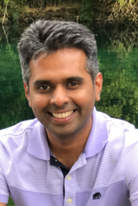 Bio: Ajay Balankutty received the B. Tech degree in electronic and communication engineering from the National Institute of Technology, Calicut, India, in 2001, and the M.S. and Ph.D. degrees in electrical engineering from Columbia University, New York, NY, in 2010.,From 2001 to 2005, he was with Analog Devices, Inc., Bangalore, India. Currently he is a Principal Engineer, leading the Serial I/O development at Intel Foundry with a focus on circuits, architecture and process technology co-optimization for next generation I/Os at Intel Foundry in Hillsboro, OR. He has published over 25 papers in peer-reviewed conferences and journals and is a member of the Technical Program Committee of CICC.
Position Statement: We are an inflection point where the demand for scaling will force use to make rapid advances that move us to the next. Electrical I/Os will continue scaling in data-rate addressing tomorrows shoreline density and per-pin bandwidth needs with low cost and high reliability, enabled by advances in circuits, packaging and connector technology, platform architectures and test capabilities. I will show some examples for 200Gb/s and 400Gb/s announcements. In the meantime, more optical integration for near-package and on-package is evolving rapidly to address the reach and scale out needed for the workloads needed for AI.
Sam Palermo, Texas A&M, USA
Position Statement: TBD
Tony Chan Carusone, University of Toronto, Alphawave, Canada
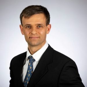 Bio: Tony Chan Carusone (S’96–M’02–SM’08–F’22) received his Ph.D. from the University of Toronto in 2002 and has since been a professor in the University of Toronto’s Department of Electrical and Computer Engineering. He has also been a consultant to industry in the areas of integrated circuit design and digital communication since 1997. He is currently the Chief Technology Officer of Alphawave Semi.
Prof. Chan Carusone has co-authored 9 Best Paper Award winners at leading conferences on wireline electrical and optical transceivers and analog integrated circuits. He co-authored the popular textbooks “Analog Integrated Circuit Design” and “Microelectronic Circuits.” He was Editor-in-Chief of the IEEE Transactions on Circuits and Systems II: Express Briefs in 2009, an Associate Editor for the IEEE Journal of Solid-State Circuits 2010-2017, and Editor-in-Chief of the IEEE Solid-State Circuits Letters 2021-2023. He was a Distinguished Lecturer for the IEEE Solid-State Circuits Society 2015-2017 and has served on the Technical Program Committee of several IEEE conferences including the International Solid-State Circuits Conference 2016-2021. He is an IEEE Fellow.
Position Statement: AI scaling is placing new, challenging demands on connectivity, and placed well-established and fundamental technology trends on a collision course. To ensure connectivity doesn’t bottleneck the performance of increasingly powerful AI accelerators, optical links will ultimately be required within racks, or even within an individual server. Given the scale of hardware roll-outs, low cost solutions are more essential then ever. However, optical solutions remain significantly (and quite fundamentally) more expensive than the copper links they are displacing. Thus, we see investments in a wide array of divergent technologies in search of a disruptive solution: higher baud rates, massive parallelism, and new material systems are all on the table.
Wednesday, 16 April
10:05 am-12:05 pm
The Impact of AI: A Job Creator or Destroyer?
As Artificial Intelligence (AI) rapidly evolves, it is transforming how we approach design, creativity, and productivity across industries. This shift brings both exciting opportunities and complex challenges to the workforce, prompting questions about the future of work. Our panel will explore critical themes, such as AI’s impact on job creation, the roles most vulnerable to automation, and the emerging opportunities that AI may create. Our expert from academia and industry will explore the unequal access to AI technology, asking whether restricted access limits innovation for smaller players and how privacy and data security concerns are evolving in an age of unprecedented data collection. Are we sacrificing too much privacy for convenience? And finally, as AI aids in brainstorming and academic work, what is its effect on research quality, creativity, and innovation?
Session Chairs:
Panelists:
Vidya Chhabria, Assistant Professor at Arizona State University, USA
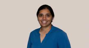 Bio: Vidya A. Chhabria is an assistant professor in the School of Electrical, Computer and Energy Engineering at Arizona State University. Her research interests lie in computer-aided design (CAD) for VLSI systems and primarily revolve around the use of AI in electronic design automation (EDA), optimization, analysis, and chip design.
John McNeill, Dean of Engineering at WPI, USA
 Bio: John McNeill is the Bernard M. Gordon Dean of Engineering at Worcester Polytechnic Institute (WPI), where he has been on the ECE faculty since 1994. He received an NSF CAREER award in 1997, WPI’s Outstanding Teaching Award in 1999, and WPI’s Exemplary Faculty Award in 2007. In 2024 he was one of WPI’s representatives to Massachusetts Governor Maura Healey’s Artificial Intelligence Task Force. He also coordinated the School of Engineering’s role in the launch of WPI’s AI Master’s program in the fall of 2024.
Position Statement: Like all new technologies, AI brings a range of possible impacts, from positive to negative. Compared to other technology introductions, perhaps most notable about AI is the vast number of fields to be impacted, and the incredibly wide range of possible visions – from utopian to dystopian.
It took years for society to be wary of social (antisocial?) media; skepticism about the benefits of AI has developed over a much shorter time frame. In the words of Todd McLees from humanskills.ai, “The more our world fills with artificial intelligence, the more it craves authentic humanity.” I will argue that we can only realize the positive benefits of AI – including improved research quality, creativity, and innovation – if we at the same time are diligent to push for a “Human First” AI centered around human thriving.
I will briefly introduce an example from my role as an engineering educator, showing how judicious use of AI in education can actually provide an experience tailored to the needs of this generation of students. AI can allow us to prioritize student needs and outcomes in developing the next wave of designers who are prepared to see AI as an opportunity of promise.
Matheus Trevisan Moreira, Tech Lead at Meta
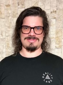 Bio: Matheus began his career as a professor in Brazil, before transitioning to the tech industry. He held key roles at startup companies, Apple, and Meta, where he is currently a tech lead. His research interests include leveraging AI technologies to aid silicon design and building architectures for next-generation AI workloads.
Position Statement: Recent advancements in generative AI have revolutionized software design and are set to transform silicon design. Large Language Models (LLMs) can understand and interact with various design collaterals, including Verilog HDL, SDC timing constraints, and CAD tool integration scripts. LLMs excel in reading natural language prompts and providing meaningful responses, enabling tasks such as code generation, log analysis, and reasoning about design choices.
By combining these capabilities with agentic workflows, we can create Gen AI agents capable of performing complex silicon design tasks autonomously or assisted by humans. This revolution will empower researchers and engineers to focus on higher-level questions, unencumbered by some monotonous and time-consuming design and verification tasks, fostering innovation. The resulting boost in creativity will lead to unprecedented innovation, as humans and their supporting Gen AI agents collaborate to devise and validate ideas, collect metrics, analyze data, and write reports.
However, a key challenge remains: the limited availability of infrastructure required to run large AI workloads, which are necessary to support these agentic workflows. Addressing this gap will be crucial to ensuring that companies and education institutions can fully leverage the transformative power of generative AI in silicon design.
Prof. Vijay Reddi, Associate Professor at Harvard, USA
 Bio: Dr. Vijay Janapa Reddi is an Associate Professor at Harvard University, specializing in computer architecture and machine learning systems. As VP and co-founder of MLCommons and board member of the Edge AI Foundations, he advances ML computing technologies. He holds a Ph.D. from Harvard and has received numerous awards.
Position Statement: Everybody wants to be an astronaut, but nobody wants to be the rocket scientist. This metaphor perfectly captures our current moment with AI. As we grapple with the panel’s central question – “The impact of AI: a job creator or destroyer?” I argue the real opportunity isn’t in predicting AI’s impact but in shaping it by developing AI engineering as a proper engineering discipline in institutions and industry, creating not just AI tools but entire ecosystems of jobs in infrastructure development, system maintenance and workforce upscaling. To that end, the debate about whether AI creates or destroys jobs misses the point. Without robust AI engineering foundations – the pipelines, testing frameworks and maintenance systems that make AI reliable and practical – most organizations can’t effectively deploy AI regardless of their aspirations. Just as the space race required not just astronauts but the entire team of engineers to succeed, realizing AI’s potential for job creation requires building a whole new engineering discipline. I’ll make the point that the key to making a force for opportunity rather than inequality isn’t just about developing better algorithms – it’s about establishing the foundations and infrastructure that can both train tomorrow’s engineers and turn promising AI technology into practical solutions. The future of work depends not just on the astronauts exploring AI’s frontier, but on developing the engineering discipline that makes the exploration possible for all.
Katy Gero, Postdoctoral Fellow at Harvard University, USA
 Bio: Katy Ilonka Gero is a human-computer interaction researcher, with a focus on creativity and writing assistants. Her work also touches on the ethics of data collection. She is a postdoc in Computer Science at Harvard University, and will be joining faculty at the University of Sydney in July, 2025.
Position Statement: There is abundant evidence, from controlled lab studies, that AI can improve ideation in a variety of contexts. However, ideation does not take place in controlled environments, and innovation requires more than good ideas. It remains unclear if AI has a significant effect when accounting for the larger context in which innovation occurs. Additionally, AI support in creative activities can change people’s sense of ownership of the resulting product and their sense of enjoyment in the process. Finally, there is evidence that while AI may improve individual ideation, it can result in homogenization across individuals. I have found in my own work on creative writing that different people find AI useful in different parts of the creative process, challenging the notion that AI will automate specific roles out of existence. I argue that AI will be picked up in research in a patchwork manner, which will then preserve heterogeneity across individuals and ensure a diverse research ecosystem.
